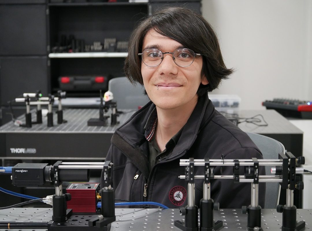
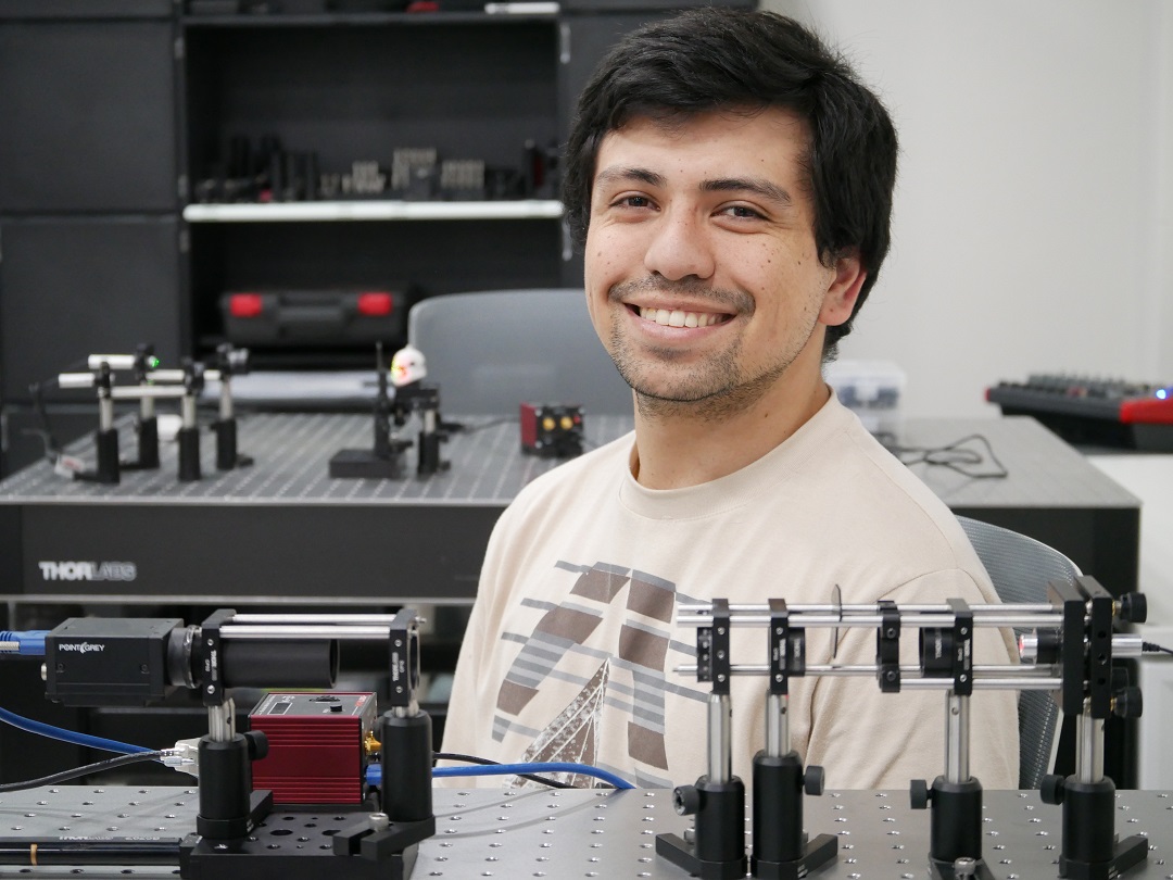
Felipe Guzmán, Electronic Civil Engineer; student of the Master program in Engineering Sciences with mention in Electrical Engineering, and assistant of the optoelectronics laboratory of the School of Electrical Engineering (SEE) of the Pontificia Universidad Católica de Valparaíso, comment to us a part of what has been his work inside the laboratory, in the field of investigation:
How do you get to work at the optoelectronics laboratory?
Felipe (F): I started working when I enrolled my undergraduate memory, on 2018. Among the topics that were offered, the development of a high-resolution microscope caught my attention. It used computational algorithms, called fourier tycography, and the guide professor was Esteban Vera.
Back then the laboratory was quite small, it was just getting started. As I was studying this area called my attention in the number of applications it has: in this case, I was working directly yo a microscope, but the math, the background, can be applied to any image system, it can be a microscope or a macroscope. It caught my attention that this area in reality until then was not very well known in the School, the optoelectronic. Along with the subjects the professor dictated, I found it attractive, so I searched for a way to dedicate myself to it.
How it has been the development with the collaboration professor Vera?
F: The professor was satisfied with the work I did, and he oriented me to present it as a paper in conferences. The first time was in Concepción, in the International Conference on Automation IEEE and Twenty-Third Congress of the Chilean Association of Automatic Control, as a advance mode of what I was working on. The second, by the end, was at the Twenty-Second Symposium on Image, Signal Processing and Artificial Vision, at the Industrial University of Santander, in Bucaramanga, Colombia.
In parallel, professor Vera suggested me to do an internship, which I did at that university, in the group of High-Dimension Signal Processing or HDSP, in English, under the tutelage of Dr. Henry Arguello, and with the orientation from the then student doctorate, Samuel Pinilla. This internship lasted three weeks. My studies were an introduction to compressive sensing, which is the specialty of the group. Apart from that, they helped me to guide me in what would become my master’s topic.
Why did you choose to enter the SEE master’s program?
F: The truth, it was a bit under the guidance of professor Vera. He advised me to continue my studies, taking advantage of the postgraduate opportunity at the School, which it allowed me to validate subjects. It was all very, very fluid, as I was finishing my undergraduate thesis and I could enter the master’s degree easily.
What are you working on right now?
F: Currently I am in my master’s thesis, which consists of using the concepts of compressive sensing that I used there (in Bucaramanga), for a camera arrangement with CMOS sensors, where I am in a planning stage, which, in fact, I have budgeted a presentation at the Sensing and Optical-Computational Images conference of the American Optical Society, which given the virus situation, we will do it online on June 1st. Only the formal presentation of my progress would remain, while the master’s thesis culminated with the publication in a specialized magazine.
How do you profile yourself professionally?
F: To get started, I like the idea of research. It is very stimulating. I particularly feel that I still have a lot to explore in optoelectronics. I have several ideas I want to try. With professor Vera and with Camilo, also a laboratory assistant, we want to do many things. We are looking to enlarge our team. I make a call to al the students and professors, that this field is coming strong, although it sounds unknown at the university, the investigations are very avant-garde. At some point, It will be become very influential.
To know more about the optoelectronics laboratory of the School of Electrical Engineering (SEE) of the Pontificia Universidad Católica de Valparaíso, you can visit the official website.


